|
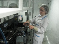
Laser multi-channel ЭМ-5189-02 image generator (IG) is used to form a topological structure on semiconductor wafers and exposure mask’s blanks. The device refers to the 5-th technology generation – technological level of 350 nm.
IG gives the opportunity to manufacture products with the help of the photolithography technology using photoresists. The area of maximum sensitivity of photoresists is near-ultraviolet region. The figure is formed by focused laser radiation with a wavelength of 355 nm.
GI forms the image on the blanks with the following requirements:
- Polished substrates size 76 mm, 100 mm;
Glass substrates for metallic exposure masks made of low and very low ratio of thermal expansion material size 27 mm (5"), 152 mm (6") 178 mm(7"), 215 (8") and thickness of 2.2 mm to 6.4 mm. OJSC “MINSK RESEARCH INSTITUTE OF RADIOMATERIALS”
Element’s edge roughness - not more than 0.3 mic;
Element’s corner rounding – not more than 0.5 mic;
Streaks junction inaccuracy – not more than ±40 nm;
The final terms and the manufacturing cost are determined in the process of preparing an order.
Back to the section
