|
There is a great variety of refused materials, which can be on different stages of semiconductor devices manufacturing.
While conducting epitaxy, photolithography or metallization or others, some parts of the wafers get rejected and can be withdrawn from the technological process. On the surface of such wafers layers of epitaxial films, photoresist, metal can be found.
OJSC “MRIR” has the technology of restoration of A3B5 wafers.
Being a part of the production process, the wafers are sorted by types of defects, the depth of the irregularities and the thickness of the plates. Then defective wafers of gallium arsenide are cleaned and got chemical surface treatment.
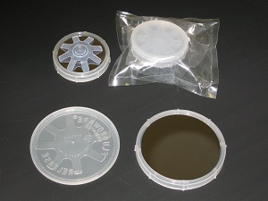
After that damaged layers are removed by chemical-mechanical polishing, precipitately surface treatment is made and wafers are packaged in individual containers with inert gas.
After that, the plate can be reused in the processes of epitaxial capacity.
If the number of recovered plates is not enough, MRIOR can produce the missing number wafers with the appropriate characteristics.
For more information, contact the marketing and sales department, phone +375 173983013, MTS +375(33)3339522.
Back to the section
